Graphene TEM Grid
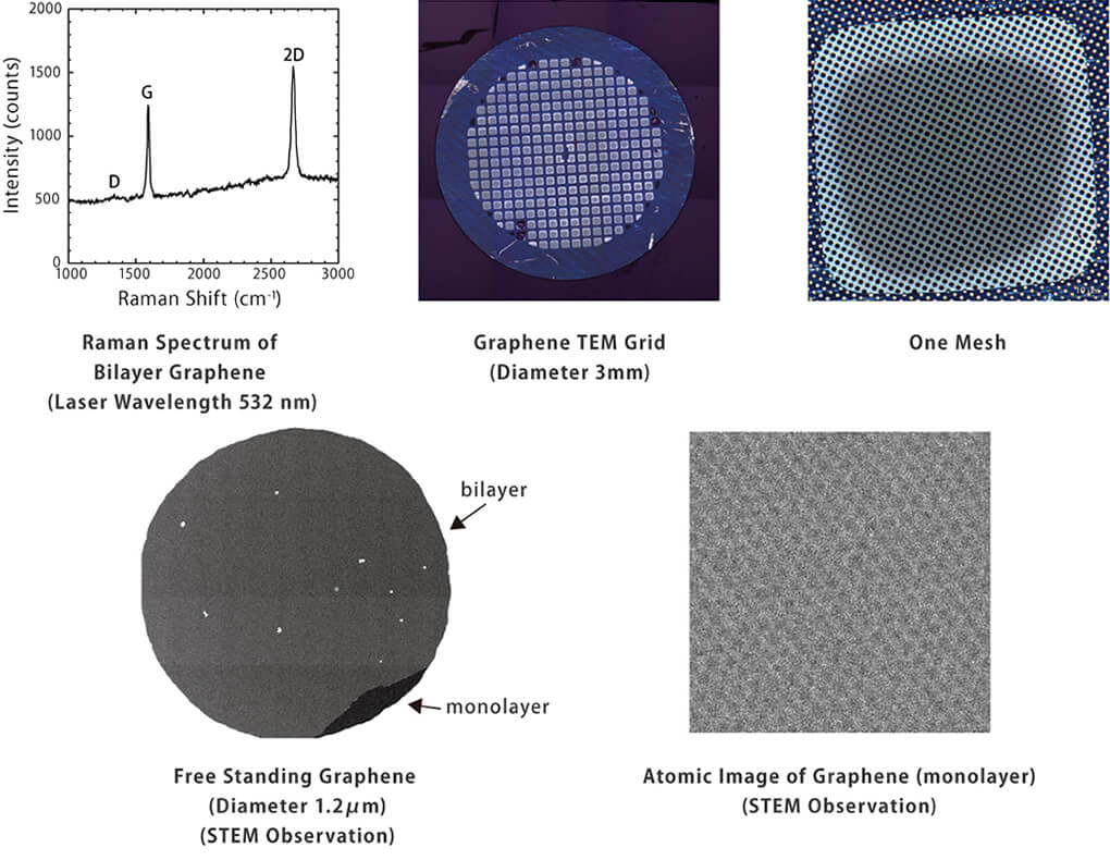
Innovative TEM grid with high-purity CVD-synthesized bilayer graphene free-standing film over grid holes.
Ideal sample support film for TEM observations of ultrafine particles, viruses, etc.
Very thin vitreous ice layer with uniform thickness, which is indispensable to cryo TEM observations,
can be formed by applying hydrophilic treatment to bilayer graphene.
We can also provide a hydrophilized graphene TEM grid.
Product Data
It is a TEM grid that uses jighly clean CVD bilayer graphene and has outstanding electron beam irradiation resistance.Also strong against hydrophilic tretment using such as UV and plasma irradiations.
Properties of Graphene
| Growth Method | Chemical Vapor Deposition(CVD)by using Cu substrate |
|---|---|
| Transfer Method | Wet Transfer by using PMMA supporting film |
| Size | 3mm(Diameter of TEM Grid) |
| Layer Number of Graphene | 1 Layer(1.0~1.4), 2 Layers (2.0~2.2) |
| Grain Size | Several μm |
| Color | Black (Transparency>95%) |
| Observation temperature range | -200~600℃ |
Substrate TEM Grid
| Type of TEM Grid | QUANTIFOIL® R 0.6/1, R1/4, R1.2/1.3 |
|---|---|
| Diameter of Free-Standing Graphene | 0.6μm(R0.6/1),1.0μm(R1/4),1.2μm(R1.2/1.3) |
| Material of TEM Grid | Mo,Au |
References
・“High-precision thickness control of ice layer on CVD grown bilayer graphene for cryo-TEM”, Carbon 160 (2020) pp107-112.